The simplest 0-30 Volt power supply for a radio amateur.
Scheme.
In this article we continue the topic of circuit design of power supplies for amateur radio laboratories. This time we will talk about the simplest device, assembled from domestically produced radio components, and with a minimum number of them.
And so, the circuit diagram of the power supply:

As you can see, everything is simple and accessible, the element base is widespread and does not contain shortages.
Let's start with the transformer. Its power should be at least 150 Watts, the voltage of the secondary winding should be 21...22 Volts, then after the diode bridge on capacitance C1 you will get about 30 Volts. Calculate so that the secondary winding can provide a current of 5 Amps.
After the step-down transformer there is a diode bridge assembled on four 10-amp D231 diodes. The current reserve is of course good, but the design is quite cumbersome. The best option would be to use an imported diode assembly of the RS602 type; with small dimensions, it is designed for a current of 6 Amps.
Electrolytic capacitors are designed for an operating voltage of 50 Volts. C1 and C3 can be set from 2000 to 6800 uF.
Zener diode D1 - it sets the upper limit for adjusting the output voltage. In the diagram we see the inscription D814D x 2, this means that D1 consists of two series-connected zener diodes D814D. The stabilization voltage of one such zener diode is 13 Volts, which means two connected in series will give us an upper limit for voltage regulation of 26 volts minus the voltage drop at the junction of transistor T1. As a result, you get smooth adjustment from zero to 25 volts.
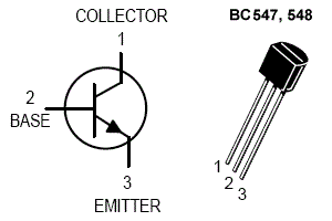
The KT819 is used as a regulating transistor in the circuit; they are available in plastic and metal cases. The location of the pins, housing dimensions and parameters of this transistor can be seen in the next two images.


Today we will assemble a laboratory power supply with our own hands. We will understand the structure of the block, select the right components, learn how to solder correctly, and assemble elements onto printed circuit boards.
This is a high-quality laboratory (and not only) power supply with variable adjustable voltage from 0 to 30 volts. The circuit also includes an electronic output current limiter that effectively regulates the output current to 2 mA from the circuit's maximum current of 3 A. This characteristic makes this power supply indispensable in the laboratory, as it makes it possible to regulate power, limit the maximum current that the connected device can consume, without fear of damage if something goes wrong.
There is also a visual indication that this limiter is in effect (LED) so you can see if your circuit is exceeding its limits.
The schematic diagram of the laboratory power supply is presented below:

Input voltage: ……………. 24 V-AC;
Input current: ……………. 3 A (max);
Output voltage: …………. 0-30 V - adjustable;
Output current: …………. 2 mA -3 A - adjustable;
Output voltage ripple: .... 0.01% maximum.
- Small size, easy to make, simple design.
— Output voltage is easily adjustable.
— Output current limitation with visual indication.
— Protection against overload and incorrect connection.
Let's start with the fact that the laboratory power supply uses a transformer with a secondary winding of 24V/3A, which is connected through input terminals 1 and 2 (the quality of the output signal is proportional to the quality of the transformer). The AC voltage from the secondary winding of the transformer is rectified by a diode bridge formed by diodes D1-D4. The ripples of the rectified DC voltage at the output of the diode bridge are smoothed by a filter formed by resistor R1 and capacitor C1. The circuit has some features that make this power supply different from other units in its class.
Instead of using feedback to control the output voltage, our circuit uses an op-amp to provide the required voltage for stable operation. This voltage drops at the output of U1. The circuit operates thanks to the D8 - 5.6 V Zener diode, which here operates at zero temperature coefficient of current. The voltage at the output of U1 drops across the diode D8 turning it on. When this happens, the circuit stabilizes and the voltage of the diode (5.6) drops across resistor R5.
The current that flows through the opera. the amplifier changes slightly, which means the same current will flow through resistors R5, R6, and since both resistors have the same voltage value, the total voltage will be summed up as if they were connected in series. Thus, the voltage obtained at the output of the opera. amplifier will be equal to 11.2 volts. Chain from oper. amplifier U2 has a constant gain of approximately 3, according to the formula A = (R11 + R12) / R11 increases the voltage of 11.2 volts to approximately 33 volts. Trimmer RV1 and resistor R10 are used to set the voltage output so that it does not drop to 0 volts, regardless of the value of other components in the circuit.
Another very important characteristic of the circuit is the ability to obtain the maximum output current that can be obtained from the p.s.u. To make this possible, the voltage drops across a resistor (R7), which is connected in series with the load. The IC responsible for this circuit function is U3. An inverted signal to input U3 equal to 0 volts is supplied through R21. At the same time, without changing the signal of the same IC, you can set any voltage value through P2. Let's say that for a given output the voltage is several volts, P2 is set so that there is a signal of 1 volt at the input of IC. If the load is amplified, the output voltage will be constant and the presence of R7 in series with the output will have little effect due to its low magnitude and due to its position outside the feedback loop of the control circuit. As long as the load and output voltage are constant, the circuit operates stably. If the load is increased so that the voltage on R7 is greater than 1 volt, U3 is turned on and stabilizes to its original parameters. U3 operates without changing the signal to U2 through D9. Thus, the voltage through R7 is constant and does not increase above a predetermined value (1 volt in our example), reducing the output voltage of the circuit. This device is capable of maintaining the output signal constant and accurate, which makes it possible to obtain 2 mA at the output.
Capacitor C8 makes the circuit more stable. Q3 is needed to control the LED whenever you use the limiter indicator. To make this possible for U2 (changing the output voltage down to 0 volts) it is necessary to provide a negative connection, which is done through the circuit C2 and C3. The same negative connection is used for U3. Negative voltage is supplied and stabilized by R3 and D7.
To avoid uncontrollable situations, there is a kind of protection circuit built around Q1. The IC is internally protected and cannot be damaged.U1 is a reference voltage source, U2 is a voltage regulator, U3 is a current stabilizer.
First of all, let's look at the basics of building electronic circuits on printed circuit boards - the basics of any laboratory power supply. The board is made of a thin insulating material covered with a thin conductive layer of copper, which is formed in such a way that the circuit elements can be connected by conductors as shown in the circuit diagram. It is necessary to design the PCB properly to avoid the device from malfunctioning. To protect the board from oxidation in the future and keep it in excellent condition, it must be coated with a special varnish that protects against oxidation and makes soldering easier.
Soldering elements into a board is the only way to assemble a laboratory power supply efficiently, and the success of your work will depend on how you do this. This is not very difficult if you follow a few rules and then you will not have any problems. The power of the soldering iron you use should not exceed 25 watts. The tip should be thin and clean throughout the entire operation. To do this, there is a damp sponge of sorts and from time to time you can clean the hot tip to remove all the residues that accumulate on it.
In order to solder the element correctly, you must do the following:
— Clean the terminals of the elements with sandpaper (preferably with a small grain).
— Bend component leads at the correct distance from the exit from the case for convenient placement on the board.
— You may encounter elements whose leads are thicker than the holes in the board. In this case, you need to widen the holes a little, but do not make them too large - this will make soldering difficult.
— The element must be inserted so that its leads protrude slightly from the surface of the board.
- When the solder melts, it will spread evenly throughout the entire area around the hole (this can be achieved by using the correct soldering iron temperature).
— Soldering one element should take no more than 5 seconds. Remove excess solder and wait until the solder on the board cools naturally (without blowing on it). If everything was done correctly, the surface should have a bright metallic tint, the edges should be smooth. If the solder appears dull, cracked, or bead-shaped, it is called dry soldering. You must delete it and do everything again. But be careful not to overheat the traces, otherwise they will lag behind the board and break easily.
— When you solder a sensitive element, you need to hold it with metal tweezers or tongs, which will absorb excess heat so as not to burn the element.
- When you complete your job, trim off the excess from the element leads and you can clean the board with alcohol to remove any remaining flux.
Before you start assembling the power supply, you need to find all the elements and divide them into groups. First, install the ICs sockets and external connections pins and solder them in place. Then resistors. Be sure to place R7 at a certain distance from the PCB as it gets very hot, especially when high current is flowing, and this can damage it. This is also recommended for R1. then place the capacitors not forgetting the polarity of the electrolytic and finally solder the diodes and transistors, but be careful not to overheat them and solder them as shown in the diagram.
Install the power transistor in the heatsink. To do this you need to follow the diagram and remember to use an insulator (mica) between the transistor body and the heatsink and a special cleaning fiber to insulate the screws from the heatsink.
Connect an insulated wire to each terminal, being careful to make a good quality connection as there is a lot of current flowing here, especially between the emitter and collector of the transistor.
Also, when assembling the power supply, it would be nice to estimate where each element will be located, in order to calculate the length of the wires that will be between the PCB and the potentiometers, the power transistor and for the input and output connections.
Connect the potentiometers, LED and power transistor and connect two pairs of ends for input and output connections. Make sure from the diagram that you are doing everything correctly, try not to confuse anything, since there are 15 external connections in the circuit and if you make a mistake, it will be difficult to find it later. It would also be a good idea to use wires of different colors.
Printed circuit board of a laboratory power supply, below there will be a link to download the signet in .lay format:

Layout of elements on the power supply board:

Connection diagram of variable resistors (potentiometers) to regulate the output current and voltage, as well as connection of the contacts of the power transistor of the power supply:

Designation of transistor and operational amplifier pins:

Terminal designations on the diagram:
— 1 and 2 to the transformer.
— 3 (+) and 4 (-) DC OUTPUT.
- 5, 10 and 12 on P1.
- 6, 11 and 13 on P2.
- 7 (E), 8 (B), 9 (E) to transistor Q4.
— LED must be installed on the outside of the board.
When all external connections are made, it is necessary to check the board and clean it to remove any remaining solder. Make sure there is no connection between adjacent tracks that could lead to a short circuit and if everything is fine, connect the transformer. And connect the voltmeter.
DO NOT TOUCH ANY PORTION OF THE CIRCUIT WHILE IT IS LIVE.
The voltmeter should show a voltage between 0 and 30 volts depending on the position of P1. Turning P2 counterclockwise should turn on the LED, indicating that our limiter is working.
R1 = 2.2 kOhm 1W
R2 = 82 Ohm 1/4W
R3 = 220 Ohm 1/4W
R4 = 4.7 kOhm 1/4W
R5, R6, R13, R20, R21 = 10 kOhm 1/4W
R7 = 0.47 Ohm 5W
R8, R11 = 27 kOhm 1/4W
R9, R19 = 2.2 kOhm 1/4W
R10 = 270 kOhm 1/4W
R12, R18 = 56kOhm 1/4W
R14 = 1.5 kOhm 1/4W
R15, R16 = 1 kOhm 1/4W
R17 = 33 Ohm 1/4W
R22 = 3.9 kOhm 1/4W
RV1 = 100K trimmer
P1, P2 = 10KOhm linear potentiometer
C1 = 3300 uF/50V electrolytic
C2, C3 = 47uF/50V electrolytic
C4 = 100nF polyester
C5 = 200nF polyester
C6 = 100pF ceramic
C7 = 10uF/50V electrolytic
C8 = 330pF ceramic
C9 = 100pF ceramic
D1, D2, D3, D4 = 1N5402,3,4 diode 2A - RAX GI837U
D5, D6 = 1N4148
D7, D8 = 5.6V Zener
D9, D10 = 1N4148
D11 = 1N4001 diode 1A
Q1 = BC548, NPN transistor or BC547
Q2 = 2N2219 NPN transistor - (Replace with KT961A- everything is working)
Q3 = BC557, PNP transistor or BC327
Q4 = 2N3055 NPN power transistor ( replace with KT 827A)
U1, U2, U3 = TL081, op. amplifier
D12 = LED diode
As a result, I assembled a laboratory power supply myself, but in practice I encountered something that I considered necessary to correct. Well, first of all, this is a power transistor Q4 = 2N3055 it urgently needs to be crossed out and forgotten. I don’t know about other devices, but it is not suitable for this regulated power supply. The fact is that this type of transistor fails instantly if there is a short circuit and the current of 3 amperes does not draw at all!!! I didn’t know what was wrong until I changed it to our native Soviet one KT 827 A. After installing it on the radiator, I didn’t know any grief and never returned to this issue.
As for the rest of the circuitry and parts, there are no difficulties. With the exception of the transformer, we had to wind it. Well, this is purely out of greed, half a bucket of them is in the corner - don’t buy it =))
Well, in order not to break the good old tradition, I am posting the result of my work to the general public 🙂 I had to play around with the column, but overall it turned out not bad:
The front panel itself - I moved the potentiometers to the left side, on the right side there was an ammeter and a voltmeter + a red LED to indicate the current limit.

The next photo shows the rear view. Here I wanted to show a method for installing a cooler with a radiator from a motherboard. A power transistor is placed on the back side of this radiator.

Here it is, the KT 827 A power transistor. Mounted on the rear wall. I had to drill holes for the legs, lubricate all contact parts with heat-conducting paste and secure them with nuts.

Here they are....the insides! Actually everything is in a heap!

Slightly larger inside the body

Front panel on the other side

Taking a closer look, you can see how the power transistor and transformer are mounted.

Power supply board on top; Here I cheated and packed low-power transistors at the bottom of the board. They are not visible here, so don't be surprised if you don't find them.

Here is the transformer. I rewound it to 25 volts of the TVS-250 output voltage. Rough, sour, not aesthetically pleasing, but everything works like a clock =) I didn’t use the second part. Left room for creativity.

Somehow like this. A little creativity and patience. The unit has been working great for 2 years now. To write this article I had to disassemble it and reassemble it. It's just awful! But everything is for you, dear readers!
Designs from our readers!
Making a power supply with your own hands makes sense not only for enthusiastic radio amateurs. A homemade power supply unit (PSU) will create convenience and save a considerable amount in the following cases:
Professional power supplies are designed to power any kind of load, incl. reactive. Possible consumers include precision equipment. The pro-BP must maintain the specified voltage with the highest accuracy for an indefinitely long time, and its design, protection and automation must allow operation by unqualified personnel in difficult conditions, for example. biologists to power their instruments in a greenhouse or on an expedition.
An amateur laboratory power supply is free from these limitations and therefore can be significantly simplified while maintaining quality indicators sufficient for personal use. Further, through also simple improvements, it is possible to obtain a special-purpose power supply from it. What are we going to do now?
Note: both SNN and ISN can operate both from an industrial frequency power supply with a transformer on iron, and from an electrical power supply.
UPSs are compact and economical. And in the pantry many people have a power supply from an old computer lying around, obsolete, but quite serviceable. So is it possible to adapt a switching power supply from a computer for amateur/working purposes? Unfortunately, a computer UPS is a rather highly specialized device and the possibilities of its use at home/at work are very limited:

It is perhaps advisable for the average amateur to use a UPS converted from a computer one only to power power tools; about this see below. The second case is if an amateur is engaged in PC repair and/or creation of logic circuits. But then he already knows how to adapt a power supply from a computer for this:
Due to the shortcomings of UPSs, plus their fundamental and circuitry complexity, we will only look at a couple of them at the end, but simple and useful, and talk about the method of repairing the IPS. The main part of the material is devoted to SNN and IPN with industrial frequency transformers. They allow a person who has just picked up a soldering iron to build a power supply of very high quality. And having it on the farm, it will be easier to master “fine” techniques.
First, let's look at the IPN. We’ll leave pulse ones in more detail until the section on repairs, but they have something in common with “iron” ones: a power transformer, a rectifier and a ripple suppression filter. Together, they can be implemented in various ways depending on the purpose of the power supply.

Pos. 1 in Fig. 1 – half-wave (1P) rectifier. The voltage drop across the diode is the smallest, approx. 2B. But the pulsation of the rectified voltage is with a frequency of 50 Hz and is “ragged”, i.e. with intervals between pulses, so the pulsation filter capacitor Sf should be 4-6 times larger in capacity than in other circuits. The use of power transformer Tr for power is 50%, because Only 1 half-wave is rectified. For the same reason, a magnetic flux imbalance occurs in the Tr magnetic circuit and the network “sees” it not as an active load, but as inductance. Therefore, 1P rectifiers are used only for low power and where there is no other way, for example. in IIN on blocking generators and with a damper diode, see below.
Note: why 2V, and not 0.7V, at which the p-n junction in silicon opens? The reason is through current, which is discussed below.
Pos. 2 – 2-half-wave with midpoint (2PS). The diode losses are the same as before. case. The ripple is 100 Hz continuous, so the smallest possible Sf is needed. Use of Tr - 100% Disadvantage - double copper consumption on the secondary winding. At the time when rectifiers were made using kenotron lamps, this did not matter, but now it is decisive. Therefore, 2PS are used in low-voltage rectifiers, mainly at higher frequencies with Schottky diodes in UPSs, but 2PS have no fundamental limitations on power.
Pos. 3 – 2-half-wave bridge, 2RM. Losses on diodes are doubled compared to pos. 1 and 2. The rest is the same as 2PS, but the secondary copper is needed almost half as much. Almost - because several turns have to be wound to compensate for the losses on a pair of “extra” diodes. The most commonly used circuit is for voltages from 12V.
Pos. 3 – bipolar. The “bridge” is depicted conventionally, as is customary in circuit diagrams (get used to it!), and is rotated 90 degrees counterclockwise, but in fact it is a pair of 2PS connected in opposite polarities, as can be clearly seen further in Fig. 6. Copper consumption is the same as 2PS, diode losses are the same as 2PM, the rest is the same as both. It is built mainly to power analog devices that require voltage symmetry: Hi-Fi UMZCH, DAC/ADC, etc.
Pos. 4 – bipolar according to the parallel doubling scheme. Provides increased voltage symmetry without additional measures, because asymmetry of the secondary winding is excluded. Using Tr 100%, ripples 100 Hz, but torn, so Sf needs double capacity. Losses on the diodes are approximately 2.7V due to the mutual exchange of through currents, see below, and at a power of more than 15-20 W they increase sharply. They are built mainly as low-power auxiliary ones for independent power supply of operational amplifiers (op-amps) and other low-power, but demanding analog components in terms of power supply quality.
In a UPS, the entire circuit is most often clearly tied to the standard size (more precisely, to the volume and cross-sectional area Sc) of the transformer/transformers, because the use of fine processes in ferrite makes it possible to simplify the circuit while making it more reliable. Here, “somehow in your own way” comes down to strict adherence to the developer’s recommendations.
The iron-based transformer is selected taking into account the characteristics of the SNN, or is taken into account when calculating it. The voltage drop across the RE Ure should not be taken less than 3V, otherwise the VS will drop sharply. As Ure increases, the VS increases slightly, but the dissipated RE power grows much faster. Therefore, Ure is taken at 4-6 V. To it we add 2(4) V of losses on the diodes and the voltage drop on the secondary winding Tr U2; for a power range of 30-100 W and voltages of 12-60 V, we take it to 2.5 V. U2 arises primarily not from the ohmic resistance of the winding (it is generally negligible in powerful transformers), but due to losses due to magnetization reversal of the core and the creation of a stray field. Simply, part of the network energy, “pumped” by the primary winding into the magnetic circuit, evaporates into outer space, which is what the value of U2 takes into account.
So, we calculated, for example, for a bridge rectifier, 4 + 4 + 2.5 = 10.5 V extra. We add it to the required output voltage of the power supply unit; let it be 12V, and divide by 1.414, we get 22.5/1.414 = 15.9 or 16V, this will be the lowest permissible voltage of the secondary winding. If TP is factory-made, we take 18V from the standard range.
Now the secondary current comes into play, which, naturally, is equal to the maximum load current. Let us say we need 3A; multiply by 18V, it will be 54W. We have obtained the overall power Tr, Pg, and we will find the rated power P by dividing Pg by the efficiency Tr η, which depends on Pg:
In our case, there will be P = 54/0.8 = 67.5 W, but there is no such standard value, so you will have to take 80 W. In order to get 12Vx3A = 36W at the output. A steam locomotive, and that's all. It’s time to learn how to calculate and wind the “trances” yourself. Moreover, in the USSR, methods for calculating transformers on iron were developed that make it possible, without loss of reliability, to squeeze 600 W out of a core, which, when calculated according to amateur radio reference books, is capable of producing only 250 W. "Iron Trance" is not as stupid as it seems.
The rectified voltage needs to be stabilized and, most often, regulated. If the load is more powerful than 30-40 W, short-circuit protection is also necessary, otherwise a malfunction of the power supply may cause a network failure. SNN does all this together.
It is better for a beginner not to immediately go into high power, but to make a simple, highly stable 12V ELV for testing according to the circuit in Fig. 2. It can then be used as a source of reference voltage (its exact value is set by R5), for checking devices, or as a high-quality ELV ION. The maximum load current of this circuit is only 40mA, but the VSC on the antediluvian GT403 and the equally ancient K140UD1 is more than 1000, and when replacing VT1 with a medium-power silicon one and DA1 on any of the modern op-amps it will exceed 2000 and even 2500. The load current will also increase to 150 -200 mA, which is already useful.

The next stage is a power supply with voltage regulation. The previous one was done according to the so-called. compensation comparison circuit, but it is difficult to convert one to a high current. We will make a new SNN based on an emitter follower (EF), in which the RE and CU are combined in just one transistor. The KSN will be somewhere around 80-150, but this will be enough for an amateur. But the SNN on the ED allows, without any special tricks, to obtain an output current of up to 10A or more, as much as the Tr will give and the RE will withstand.

The circuit of a simple 0-30V power supply is shown in pos. 1 Fig. 3. IPN for it is a ready-made transformer such as TPP or TS for 40-60 W with a secondary winding for 2x24V. Rectifier type 2PS with diodes rated at 3-5A or more (KD202, KD213, D242, etc.). VT1 is installed on a radiator with an area of 50 square meters or more. cm; An old PC processor will work very well. Under such conditions, this ELV is not afraid of a short circuit, only VT1 and Tr will heat up, so a 0.5A fuse in the primary winding circuit of Tr is enough for protection.
Pos. Figure 2 shows how convenient a power supply on an electric power supply is for an amateur: there is a 5A power supply circuit with adjustment from 12 to 36 V. This power supply can supply 10A to the load if there is a 400W 36V Tr. Its first feature is the integrated SNN K142EN8 (preferably with index B) acts in an unusual role as a control unit: to its own 12V output is added, partially or completely, all 24V, the voltage from the ION to R1, R2, VD5, VD6. Capacitors C2 and C3 prevent excitation on HF DA1 operating in an unusual mode.
The next point is the short circuit protection device (PD) on R3, VT2, R4. If the voltage drop across R4 exceeds approximately 0.7V, VT2 will open, close the base circuit of VT1 to the common wire, it will close and disconnect the load from the voltage. R3 is needed so that the extra current does not damage DA1 when the ultrasound is triggered. There is no need to increase its denomination, because when the ultrasound is triggered, you need to securely lock VT1.
And the last thing is the seemingly excessive capacitance of the output filter capacitor C4. In this case it is safe, because The maximum collector current of VT1 of 25A ensures its charge when turned on. But this ELV can supply a current of up to 30A to the load within 50-70 ms, so this simple power supply is suitable for powering low-voltage power tools: its starting current does not exceed this value. You just need to make (at least from plexiglass) a contact block-shoe with a cable, put on the heel of the handle, and let the “Akumych” rest and save resources before leaving.
Let's say in this circuit the output is 12V with a maximum of 5A. This is just the average power of a jigsaw, but, unlike a drill or screwdriver, it takes it all the time. At C1 it stays at about 45V, i.e. on RE VT1 it remains somewhere around 33V at a current of 5A. Power dissipation is more than 150 W, even more than 160, if you consider that VD1-VD4 also needs to be cooled. It is clear from this that any powerful adjustable power supply must be equipped with a very effective cooling system.

A finned/needle radiator using natural convection does not solve the problem: calculations show that a dissipating surface of 2000 sq. m. is needed. see and the thickness of the radiator body (the plate from which the fins or needles extend) is from 16 mm. To own this much aluminum in a shaped product was and remains a dream in a crystal castle for an amateur. A CPU cooler with airflow is also not suitable; it is designed for less power.
One of the options for the home craftsman is an aluminum plate with a thickness of 6 mm and dimensions of 150x250 mm with holes of increasing diameter drilled along the radii from the installation site of the cooled element in a checkerboard pattern. It will also serve as the rear wall of the power supply housing, as in Fig. 4.
An indispensable condition for the effectiveness of such a cooler is a weak, but continuous flow of air through the perforations from the outside to the inside. To do this, install a low-power exhaust fan in the housing (preferably at the top). A computer with a diameter of 76 mm or more is suitable, for example. add. HDD cooler or video card. It is connected to pins 2 and 8 of DA1, there is always 12V.
Note: In fact, a radical way to overcome this problem is a secondary winding Tr with taps for 18, 27 and 36V. The primary voltage is switched depending on which tool is being used.
The described power supply for the workshop is good and very reliable, but it’s hard to carry it with you on trips. This is where a computer power supply will fit in: the power tool is insensitive to most of its shortcomings. Some modification most often comes down to installing an output (closest to the load) electrolytic capacitor of large capacity for the purpose described above. There are a lot of recipes for converting computer power supplies for power tools (mainly screwdrivers, which are not very powerful, but very useful) in RuNet; one of the methods is shown in the video below, for a 12V tool.
With 18V tools it’s even easier: for the same power they consume less current. A much more affordable ignition device (ballast) from a 40 W or more energy saving lamp may be useful here; it can be completely placed in the case of a bad battery, and only the cable with the power plug will remain outside. How to make a power supply for an 18V screwdriver from ballast from a burnt housekeeper, see the following video.
But let’s return to SNN on ES; their capabilities are far from being exhausted. In Fig. 5 – bipolar powerful power supply with 0-30 V regulation, suitable for Hi-Fi audio equipment and other fastidious consumers. The output voltage is set using one knob (R8), and the symmetry of the channels is maintained automatically at any voltage value and any load current. A pedant-formalist may turn gray before his eyes when he sees this circuit, but the author has had such a power supply working properly for about 30 years.

The main stumbling block during its creation was δr = δu/δi, where δu and δi are small instantaneous increments of voltage and current, respectively. To develop and set up high-quality equipment, it is necessary that δr does not exceed 0.05-0.07 Ohm. Simply, δr determines the ability of the power supply to instantly respond to surges in current consumption.
For the SNN on the EP, δr is equal to that of the ION, i.e. zener diode divided by the current transfer coefficient β RE. But for powerful transistors, β drops significantly at a large collector current, and δr of a zener diode ranges from a few to tens of ohms. Here, in order to compensate for the voltage drop across the RE and reduce the temperature drift of the output voltage, we had to assemble a whole chain of them in half with diodes: VD8-VD10. Therefore, the reference voltage from the ION is removed through an additional ED on VT1, its β is multiplied by β RE.
The next feature of this design is short circuit protection. The simplest one, described above, does not fit into a bipolar circuit in any way, so the protection problem is solved according to the principle “there is no trick against scrap”: there is no protective module as such, but there is redundancy in the parameters of powerful elements - KT825 and KT827 at 25A and KD2997A at 30A. T2 is not capable of providing such a current, and while it warms up, FU1 and/or FU2 will have time to burn out.
Note: It is not necessary to indicate blown fuses on miniature incandescent lamps. It’s just that at that time LEDs were still quite scarce, and there were several handfuls of SMOKs in the stash.
It remains to protect the RE from the extra discharge currents of the pulsation filter C3, C4 during a short circuit. To do this, they are connected through low-resistance limiting resistors. In this case, pulsations may appear in the circuit with a period equal to the time constant R(3,4)C(3,4). They are prevented by C5, C6 of smaller capacity. Their extra currents are no longer dangerous for RE: the charge drains faster than the crystals of the powerful KT825/827 heat up.
Output symmetry is ensured by op-amp DA1. The RE of the negative channel VT2 is opened by current through R6. As soon as the minus of the output exceeds the plus in absolute value, it will slightly open VT3, which will close VT2 and the absolute values of the output voltages will be equal. Operational control over the symmetry of the output is carried out using a dial gauge with a zero in the middle of the scale P1 (its appearance is shown in the inset), and adjustment, if necessary, is carried out by R11.
The last highlight is the output filter C9-C12, L1, L2. This design is necessary to absorb possible HF interference from the load, so as not to rack your brain: the prototype is buggy or the power supply is “wobbly”. With electrolytic capacitors alone, shunted with ceramics, there is no complete certainty here; the large self-inductance of the “electrolytes” interferes. And chokes L1, L2 divide the “return” of the load across the spectrum, and to each their own.
This power supply unit, unlike the previous ones, requires some adjustment:
PSUs fail more often than other electronic devices: they take the first blow of network surges, and they also get a lot from the load. Even if you do not intend to make your own power supply, a UPS can be found, in addition to a computer, in a microwave oven, washing machine, and other household appliances. The ability to diagnose a power supply and knowledge of the basics of electrical safety will make it possible, if not to fix the fault yourself, then to competently bargain on the price with repairmen. Therefore, let's look at how a power supply is diagnosed and repaired, especially with an IIN, because over 80% of failures are their share.

First of all, about some effects, without understanding which it is impossible to work with a UPS. The first of them is the saturation of ferromagnets. They are not capable of absorbing energies of more than a certain value, depending on the properties of the material. Hobbyists rarely encounter saturation on iron; it can be magnetized to several Tesla (Tesla, a unit of measurement of magnetic induction). When calculating iron transformers, the induction is taken to be 0.7-1.7 Tesla. Ferrites can withstand only 0.15-0.35 T, their hysteresis loop is “more rectangular”, and operate at higher frequencies, so their probability of “jumping into saturation” is orders of magnitude higher.
If the magnetic circuit is saturated, the induction in it no longer grows and the EMF of the secondary windings disappears, even if the primary has already melted (remember school physics?). Now turn off the primary current. The magnetic field in soft magnetic materials (hard magnetic materials are permanent magnets) cannot exist stationary, like an electric charge or water in a tank. It will begin to dissipate, the induction will drop, and an EMF of the opposite polarity relative to the original polarity will be induced in all windings. This effect is quite widely used in IIN.
Unlike saturation, through current in semiconductor devices (simply draft) is an absolutely harmful phenomenon. It arises due to the formation/resorption of space charges in the p and n regions; for bipolar transistors - mainly in the base. Field-effect transistors and Schottky diodes are practically free from drafts.
For example, when voltage is applied/removed to a diode, it conducts current in both directions until the charges are collected/dissolved. That is why the voltage loss on the diodes in rectifiers is more than 0.7V: at the moment of switching, part of the charge of the filter capacitor has time to flow through the winding. In a parallel doubling rectifier, the draft flows through both diodes at once.
A draft of transistors causes a voltage surge on the collector, which can damage the device or, if a load is connected, damage it through extra current. But even without that, a transistor draft increases dynamic energy losses, like a diode draft, and reduces the efficiency of the device. Powerful field-effect transistors are almost not susceptible to it, because do not accumulate charge in the base due to its absence, and therefore switch very quickly and smoothly. “Almost”, because their source-gate circuits are protected from reverse voltage by Schottky diodes, which are slightly, but through.
UPS trace their origins to the blocking generator, pos. 1 in Fig. 6. When turned on, Uin VT1 is slightly opened by current through Rb, current flows through winding Wk. It cannot instantly grow to the limit (remember school physics again); an emf is induced in the base Wb and load winding Wn. From Wb, through Sb, it forces the unlocking of VT1. No current flows through Wn yet and VD1 does not start up.

When the magnetic circuit is saturated, the currents in Wb and Wn stop. Then, due to the dissipation (resorption) of energy, the induction drops, an EMF of the opposite polarity is induced in the windings, and the reverse voltage Wb instantly locks (blocks) VT1, saving it from overheating and thermal breakdown. Therefore, such a scheme is called a blocking generator, or simply blocking. Rk and Sk cut off HF interference, of which blocking produces more than enough. Now some useful power can be removed from Wn, but only through the 1P rectifier. This phase continues until the Sat is completely recharged or until the stored magnetic energy is exhausted.
This power, however, is small, up to 10W. If you try to take more, VT1 will burn out from a strong draft before it locks. Since Tp is saturated, the blocking efficiency is no good: more than half of the energy stored in the magnetic circuit flies away to warm other worlds. True, due to the same saturation, blocking to some extent stabilizes the duration and amplitude of its pulses, and its circuit is very simple. Therefore, blocking-based TINs are often used in cheap phone chargers.
Note: the value of Sb largely, but not completely, as they write in amateur reference books, determines the pulse repetition period. The value of its capacitance must be linked to the properties and dimensions of the magnetic circuit and the speed of the transistor.
Blocking at one time gave rise to line scan TVs with cathode ray tubes (CRT), and it gave birth to an INN with a damper diode, pos. 2. Here the control unit, based on signals from Wb and the DSP feedback circuit, forcibly opens/locks VT1 before Tr is saturated. When VT1 is locked, the reverse current Wk is closed through the same damper diode VD1. This is the working phase: already greater than in blocking, part of the energy is removed into the load. It’s big because when it’s completely saturated, all the extra energy flies away, but here there’s not enough of that extra. In this way it is possible to remove power up to several tens of watts. However, since the control device cannot operate until Tr has approached saturation, the transistor still shows through strongly, the dynamic losses are large and the efficiency of the circuit leaves much more to be desired.
The IIN with a damper is still alive in televisions and CRT displays, since in them the IIN and the horizontal scan output are combined: the power transistor and TP are common. This greatly reduces production costs. But, frankly speaking, an IIN with a damper is fundamentally stunted: the transistor and transformer are forced to work all the time on the verge of failure. The engineers who managed to bring this circuit to acceptable reliability deserve the deepest respect, but it is strongly not recommended to stick a soldering iron in there except for professionals who have undergone professional training and have the appropriate experience.
The push-pull INN with a separate feedback transformer is most widely used, because has the best quality indicators and reliability. However, in terms of RF interference, it also sins terribly in comparison with “analog” power supplies (with transformers on hardware and SNN). Currently, this scheme exists in many modifications; powerful bipolar transistors in it are almost completely replaced by field-effect ones controlled by special devices. IC, but the principle of operation remains unchanged. It is illustrated by the original diagram, pos. 3.
The limiting device (LD) limits the charging current of the capacitors of the input filter Sfvkh1(2). Their large size is an indispensable condition for the operation of the device, because During one operating cycle, a small fraction of the stored energy is taken from them. Roughly speaking, they play the role of a water tank or air receiver. When charging “short”, the extra charge current can exceed 100A for a time of up to 100 ms. Rc1 and Rc2 with a resistance of the order of MOhm are needed to balance the filter voltage, because the slightest imbalance of his shoulders is unacceptable.
When Sfvkh1(2) are charged, the ultrasonic trigger device generates a trigger pulse that opens one of the arms (which one does not matter) of the inverter VT1 VT2. A current flows through the winding Wk of a large power transformer Tr2 and the magnetic energy from its core through the winding Wn is almost completely spent on rectification and on the load.
A small part of the energy Tr2, determined by the value of Rogr, is removed from the winding Woc1 and supplied to the winding Woc2 of a small basic feedback transformer Tr1. It quickly saturates, the open arm closes and, due to dissipation in Tr2, the previously closed one opens, as described for blocking, and the cycle repeats.
In essence, a push-pull IIN is 2 blockers “pushing” each other. Since the powerful Tr2 is not saturated, the draft VT1 VT2 is small, completely “sinks” into the magnetic circuit Tr2 and ultimately goes into the load. Therefore, a two-stroke IPP can be built with a power of up to several kW.
It's worse if he ends up in XX mode. Then, during the half cycle, Tr2 will have time to saturate itself and a strong draft will burn both VT1 and VT2 at once. However, now there are power ferrites on sale for induction up to 0.6 Tesla, but they are expensive and degrade from accidental magnetization reversal. Ferrites with a capacity of more than 1 Tesla are being developed, but in order for IINs to achieve “iron” reliability, at least 2.5 Tesla is needed.
When troubleshooting an “analog” power supply, if it is “stupidly silent,” first check the fuses, then the protection, RE and ION, if it has transistors. They ring normally - we move on element by element, as described below.
In the IIN, if it “starts up” and immediately “stalls out”, they first check the control unit. The current in it is limited by a powerful low-resistance resistor, then shunted by an optothyristor. If the “resistor” is apparently burnt, replace it and the optocoupler. Other elements of the control device fail extremely rarely.
If the IIN is “silent, like a fish on ice,” the diagnosis also begins with the OU (maybe the “rezik” has completely burned out). Then - ultrasound. Cheap models use transistors in avalanche breakdown mode, which is far from being very reliable.
The next stage in any power supply is electrolytes. Fracture of the housing and leakage of electrolyte are not nearly as common as they write on the RuNet, but loss of capacity occurs much more often than failure of active elements. Electrolytic capacitors are checked with a multimeter capable of measuring capacitance. Below the nominal value by 20% or more - we lower the “dead” into the sludge and install a new, good one.

Then there are the active elements. You probably know how to dial diodes and transistors. But there are 2 tricks here. The first is that if a Schottky diode or zener diode is called by a tester with a 12V battery, then the device may show a breakdown, although the diode is quite good. It is better to call these components using a pointer device with a 1.5-3 V battery.
The second is powerful field workers. Above (did you notice?) it is said that their I-Z are protected by diodes. Therefore, powerful field-effect transistors seem to sound like serviceable bipolar transistors, even if they are unusable if the channel is “burnt out” (degraded) not completely.
Here, the only way available at home is to replace them with known good ones, both at once. If there is a burnt one left in the circuit, it will immediately pull a new working one with it. Electronics engineers joke that powerful field workers cannot live without each other. Another prof. joke – “replacement gay couple.” This means that the transistors of the IIN arms must be strictly of the same type.
Finally, film and ceramic capacitors. They are characterized by internal breaks (found by the same tester that checks the “air conditioners”) and leakage or breakdown under voltage. To “catch” them, you need to assemble a simple circuit according to Fig. 7. Step-by-step testing of electrical capacitors for breakdown and leakage is carried out as follows:

This is where the methodological part of the diagnosis ends and the creative part begins, where all the instructions are based on your own knowledge, experience and considerations.
UPSs are a special article due to their complexity and circuit diversity. Here, to begin with, we will look at a couple of samples using pulse width modulation (PWM), which allows us to obtain the best quality UPS. There are a lot of PWM circuits in RuNet, but PWM is not as scary as it is made out to be...
You can simply light the LED strip from any power supply described above, except for the one in Fig. 1, setting the required voltage. SNN with pos. 1 Fig. 3, it’s easy to make 3 of these, for channels R, G and B. But the durability and stability of the LEDs’ glow does not depend on the voltage applied to them, but on the current flowing through them. Therefore, a good power supply for LED strip should include a load current stabilizer; in technical terms - a stable current source (IST).

One of the schemes for stabilizing the light strip current, which can be repeated by amateurs, is shown in Fig. 8. It is assembled on an integrated timer 555 (domestic analogue - K1006VI1). Provides a stable tape current from a power supply voltage of 9-15 V. The amount of stable current is determined by the formula I = 1/(2R6); in this case - 0.7A. The powerful transistor VT3 is necessarily a field-effect transistor; from a draft, due to the base charge, a bipolar PWM simply will not form. Inductor L1 is wound on a ferrite ring 2000NM K20x4x6 with a 5xPE 0.2 mm harness. Number of turns – 50. Diodes VD1, VD2 – any silicon RF (KD104, KD106); VT1 and VT2 – KT3107 or analogues. With KT361, etc. The input voltage and brightness control ranges will decrease.
The circuit works like this: first, the time-setting capacitance C1 is charged through the R1VD1 circuit and discharged through VD2R3VT2, open, i.e. in saturation mode, through R1R5. The timer generates a sequence of pulses with the maximum frequency; more precisely - with a minimum duty cycle. The VT3 inertia-free switch generates powerful impulses, and its VD3C4C3L1 harness smooths them out to direct current.
Note: The duty cycle of a series of pulses is the ratio of their repetition period to the pulse duration. If, for example, the pulse duration is 10 μs, and the interval between them is 100 μs, then the duty cycle will be 11.
The current in the load increases, and the voltage drop across R6 opens VT1, i.e. transfers it from the cut-off (locking) mode to the active (reinforcing) mode. This creates a leakage circuit for the base of VT2 R2VT1+Upit and VT2 also goes into active mode. The discharge current C1 decreases, the discharge time increases, the duty cycle of the series increases and the average current value drops to the norm specified by R6. This is the essence of PWM. At minimum current, i.e. at maximum duty cycle, C1 is discharged through the VD2-R4-internal timer switch circuit.
In the original design, the ability to quickly adjust the current and, accordingly, the brightness of the glow is not provided; There are no 0.68 ohm potentiometers. The easiest way to adjust the brightness is by connecting, after adjustment, a 3.3-10 kOhm potentiometer R* into the gap between R3 and the VT2 emitter, highlighted in brown. By moving its engine down the circuit, we will increase the discharge time of C4, the duty cycle and reduce the current. Another method is to bypass the base junction of VT2 by turning on a potentiometer of approximately 1 MOhm at points a and b (highlighted in red), less preferable, because the adjustment will be deeper, but rougher and sharper.
Unfortunately, to set up this useful not only for IST light tapes, you need an oscilloscope:
In Fig. 9 – diagram of the simplest ISN with PWM, suitable for charging a phone, smartphone, tablet (a laptop, unfortunately, will not work) from a homemade solar battery, wind generator, motorcycle or car battery, magneto flashlight “bug” and other low-power unstable random sources power supply See the diagram for the input voltage range, there is no error there. This ISN is indeed capable of producing an output voltage greater than the input. As in the previous one, here there is the effect of changing the polarity of the output relative to the input; this is generally a proprietary feature of PWM circuits. Let's hope that after reading the previous one carefully, you will understand the work of this tiny little thing yourself.

Charging batteries is a very complex and delicate physical and chemical process, the violation of which reduces their service life several times or tens of times, i.e. number of charge-discharge cycles. The charger must, based on very small changes in battery voltage, calculate how much energy has been received and regulate the charging current accordingly according to a certain law. Therefore, the charger is by no means a power supply, and only batteries in devices with a built-in charge controller can be charged from ordinary power supplies: phones, smartphones, tablets, and certain models of digital cameras. And charging, which is a charger, is a subject for a separate discussion.
Question-remont.ru said:
There will be some sparking from the rectifier, but it's probably not a big deal. The point is the so-called. differential output impedance of the power supply. For alkaline batteries it is about mOhm (milliohms), for acid batteries it is even less. A trance with a bridge without smoothing has tenths and hundredths of an ohm, i.e. approx. 100 – 10 times more. And the starting current of a brushed DC motor can be 6-7 or even 20 times greater than the operating current. Yours is most likely closer to the latter - fast-accelerating motors are more compact and more economical, and the huge overload capacity of the batteries allows you to give the engine as much current as it can handle. for acceleration. A trans with a rectifier will not provide as much instantaneous current, and the engine accelerates more slowly than it was designed for, and with a large slip of the armature. From this, from the large slip, a spark arises, and then remains in operation due to self-induction in the windings.
What can I recommend here? First: take a closer look - how does it spark? You need to watch it in operation, under load, i.e. during sawing.
If sparks dance in certain places under the brushes, it’s okay. My powerful Konakovo drill sparkles so much from birth, and for goodness sake. In 24 years, I changed the brushes once, washed them with alcohol and polished the commutator - that’s all. If you connected an 18V instrument to a 24V output, then a little sparking is normal. Unwind the winding or extinguish the excess voltage with something like a welding rheostat (a resistor of approximately 0.2 Ohm for a power dissipation of 200 W or more), so that the motor operates at the rated voltage and, most likely, the spark will go away. If you connected it to 12 V, hoping that after rectification it would be 18, then in vain - the rectified voltage drops significantly under load. And the commutator electric motor, by the way, doesn’t care whether it is powered by direct current or alternating current.
Specifically: take 3-5 m of steel wire with a diameter of 2.5-3 mm. Roll into a spiral with a diameter of 100-200 mm so that the turns do not touch each other. Place on a fireproof dielectric pad. Clean the ends of the wire until shiny and fold them into “ears”. It is best to immediately lubricate with graphite lubricant to prevent oxidation. This rheostat is connected to the break in one of the wires leading to the instrument. It goes without saying that the contacts should be screws, tightened tightly, with washers. Connect the entire circuit to the 24V output without rectification. The spark is gone, but the power on the shaft has also dropped - the rheostat needs to be reduced, one of the contacts needs to be switched 1-2 turns closer to the other. It still sparks, but less - the rheostat is too small, you need to add more turns. It is better to immediately make the rheostat obviously large so as not to screw on additional sections. It’s worse if the fire is along the entire line of contact between the brushes and the commutator or spark tails trail behind them. Then the rectifier needs an anti-aliasing filter somewhere, according to your data, from 100,000 µF. Not a cheap pleasure. The “filter” in this case will be an energy storage device for accelerating the motor. But it may not help if the overall power of the transformer is not enough. Efficiency of brushed DC motors is approx. 0.55-0.65, i.e. trans is needed from 800-900 W. That is, if the filter is installed, but still sparks with fire under the entire brush (under both, of course), then the transformer is not up to the task. Yes, if you install a filter, then the diodes of the bridge must be rated for triple the operating current, otherwise they may fly out from the surge of charging current when connected to the network. And then the tool can be launched 5-10 seconds after being connected to the network, so that the “banks” have time to “pump up”.
And the worst thing is if the tails of sparks from the brushes reach or almost reach the opposite brush. This is called all-round fire. It very quickly burns out the collector to the point of complete disrepair. There can be several reasons for a circular fire. In your case, the most probable is that the motor was turned on at 12 V with rectification. Then, at a current of 30 A, the electrical power in the circuit is 360 W. The anchor slides more than 30 degrees per revolution, and this is necessarily a continuous all-round fire. It is also possible that the motor armature is wound with a simple (not double) wave. Such electric motors are better at overcoming instantaneous overloads, but they have a starting current - mother, don’t worry. I can’t say more precisely in absentia, and there’s no point in it – there’s hardly anything we can fix here with our own hands. Then it will probably be cheaper and easier to find and purchase new batteries. But first, try turning on the engine at a slightly higher voltage through the rheostat (see above). Almost always, in this way it is possible to shoot down a continuous all-round fire at the cost of a small (up to 10-15%) reduction in power on the shaft.
Every radio amateur, whether he is a beginner or even a professional, should have a power supply on the edge of his desk. I currently have two power supplies on my desk. One produces a maximum of 15 Volts and 1 Ampere (black arrow), and the other 30 Volts, 5 Amps (right):
Well, there is also a self-made power supply:

I think you have often seen them in my experiments, which I showed in various articles.
I bought factory power supplies a long time ago, so they didn’t cost me much. But, at the present time, when this article is being written, the dollar is already breaking through the 70 ruble mark. The crisis, motherfucker, has everyone and everything.
Okay, something went wrong... So what am I talking about? Oh yes! I think not everyone’s pockets are bursting with money... Then why don’t we put together a simple and reliable power supply circuit with our own hands, which will be no worse than a purchased unit? Actually, that’s what our reader did. I dug up a schematic and assembled the power supply myself:

It turned out very well! So, further on his behalf...
First of all, let's figure out what this power supply is good at:
– output voltage can be adjusted in the range from 0 to 30 Volts
– you can set a current limit of up to 3 Amperes, after which the unit goes into protection (a very convenient function, those who have used it know).
– very low ripple level (the direct current at the output of the power supply is not much different from the direct current of batteries and accumulators)
– protection against overload and incorrect connection
– on the power supply, by short circuiting the “crocodiles”, the maximum permissible current is set. Those. current limit, which you set with a variable resistor using an ammeter. Therefore, overloads are not dangerous. An indicator (LED) will light up indicating that the set current level has been exceeded.
So, now first things first. The diagram has been circulating on the Internet for a long time (click on the image, it will open in a new window in full screen):

The numbers in circles are contacts to which you need to solder wires that will go to radio elements.
Designation of circles in the diagram:
- 1 and 2 to the transformer.
- 3 (+) and 4 (-) DC output.
- 5, 10 and 12 on P1.
- 6, 11 and 13 on P2.
- 7 (K), 8 (B), 9 (E) to transistor Q4.
Inputs 1 and 2 are supplied with 24 Volt alternating voltage from the mains transformer. The transformer must be of decent size so that it can deliver up to 3 Amperes to the load lightly. You can buy it, or you can wind it).
Diodes D1...D4 are connected into a diode bridge. You can take diodes 1N5401...1N5408 or some others that can withstand direct current up to 3 Amps and higher. You can also use a ready-made diode bridge, which would also withstand direct current up to 3 Amps and higher. I used KD213 tablet diodes:

Microcircuits U1, U2, U3 are operational amplifiers. Here is their pinout (location of pins). View from above:

The eighth pin says “NC”, which means that this pin does not need to be connected anywhere. Neither a minus nor a plus of nutrition. In the circuit, pins 1 and 5 also do not connect anywhere.
Transistor Q1 brand BC547 or BC548. Below is its pinout:
Transistor Q2 is better to take a Soviet one, brand KT961A

Don't forget to put it on the radiator.
Transistor Q3 brand BC557 or BC327

Transistor Q4 must be KT827!

Here is its pinout:

I did not redraw the circuit, so there are elements that can lead to confusion - these are variable resistors. Since the power supply circuit is Bulgarian, their variable resistors are designated as follows:
Here we have it:

I even indicated how to find out its conclusions by rotating the column (twist).
Well, actually, the list of elements:
R1 = 2.2 kOhm 1W
R2 = 82 Ohm 1/4W
R3 = 220 Ohm 1/4W
R4 = 4.7 kOhm 1/4W
R5, R6, R13, R20, R21 = 10 kOhm 1/4W
R7 = 0.47 Ohm 5W
R8, R11 = 27 kOhm 1/4W
R9, R19 = 2.2 kOhm 1/4W
R10 = 270 kOhm 1/4W
R12, R18 = 56kOhm 1/4W
R14 = 1.5 kOhm 1/4W
R15, R16 = 1 kOhm 1/4W
R17 = 33 Ohm 1/4W
R22 = 3.9 kOhm 1/4W
RV1 = 100K multi-turn trimmer resistor
P1, P2 = 10KOhm linear potentiometer
C1 = 3300 uF/50V electrolytic
C2, C3 = 47uF/50V electrolytic
C4 = 100nF
C5 = 200nF
C6 = 100pF ceramic
C7 = 10uF/50V electrolytic
C8 = 330pF ceramic
C9 = 100pF ceramic
D1, D2, D3, D4 = 1N5401…1N5408
D5, D6 = 1N4148
D7, D8 = zener diodes at 5.6V
D9, D10 = 1N4148
D11 = 1N4001 diode 1A
Q1 = BC548 or BC547
Q2 = KT961A
Q3 = BC557 or BC327
Q4 = KT 827A
U1, U2, U3 = TL081, operational amplifier
D12 = LED
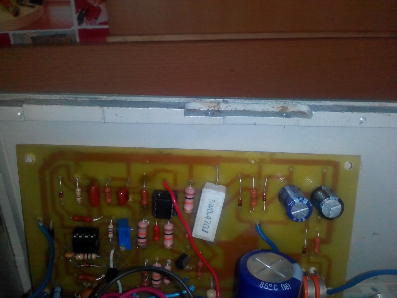
Now I will tell you how I collected it. The transformer was already taken ready from the amplifier. The voltage at its outputs was about 22 Volts. Then I began to prepare the case for my PSU (power supply)

etched


washed the toner

drilled holes:

I soldered the beds for the op-amps (operational amplifiers) and all other radio elements, except for two powerful transistors (they will lie on the radiator) and variable resistors:

And this is what the board looks like when fully assembled:

We prepare a place for a scarf in our building:
Attaching the radiator to the body:

Don't forget about the cooler that will cool our transistors:

Well, after the plumbing work I got a very nice power supply. So what do you think?

I took the job description, signet and list of radio elements at the end of the article.
Well, if anyone is too lazy to bother, then you can always buy a similar kit of this circuit for pennies on Aliexpress at this link


A schematic diagram of an easy-to-manufacture stabilized and powerful power supply with an adjustable output voltage from 5V to 35V and a load current of 5A, 10A, 20A, 30A, 40A and more (depending on the number of microcircuits) is presented.
The power supply can provide currents up to 5A (one chip), 10A (two chips), 20A (4 pcs), 30 A (6 pcs), 40 A (8 pcs), etc. The voltage can be adjusted, for example, you can set frequently used voltages to 5V, 12V, 24V, 28V, 30V and others.
The power supply is based on powerful integrated stabilizers LM338, each of which can provide an output current of up to 5A at a voltage of 1.2 to 35V (data from the datasheet).
Rice. 1. Schematic diagram of a powerful power supply for voltage 5V-30V and current 5A, 10A, 20A, 30A and more.
The secondary winding of the power transformer must produce an alternating voltage with a value of at least 18-25V. It is advisable to select the power of the transformer with a reserve, depending on the required voltage and current at the output of the future power supply.
The BD140 transistor needs to be installed on a small radiator. All LM338 integrated stabilizers must be installed on separate radiators of sufficient area for reliable heat dissipation.

Rice. 2. Appearance of powerful integrated stabilizers LM338.

Rice. 3. Pinout (pin arrangement) for LM338 microcircuits.
All powerful chips can be installed on one common heatsink through mica spacers, since the chip packages do not have to be connected together.
The current supplied at the output of the power supply can be increased or decreased, respectively, by adding or decreasing the number of “LM338 stabilizer + Rx resistor” pairs used.
You can apply active cooling to the radiator - install a small fan from the computer, supplying it with power through a 5-12V stabilizer (7805, 7812), this will reduce the size of the radiator and increase the efficiency of heat removal.
The diode bridge can be used ready-made for the required current, or it can be assembled from four separate powerful diodes (D1-D4). These diodes must be designed for the current that is planned to be received at the output of the stabilizer.
![]()
Rice. 4. Pinout of transistor BD140 (P-N-P).
For example, a diode bridge consisting of four D242 rectifier diodes will provide operating currents of up to 10A. It is advisable to install diodes or a diode bridge on a separate small radiator.
As resistors R3, R4...Rx, you can install ceramic cement ones or use wire ones, since each such resistor will dissipate approximately 4-7 Watts of power (depending on the total load on the stabilizer).
Alexander sent us the PCB layout in Sprint Layout 6 format. There is no capacitor C4 on it - we solder it to the terminals of the variable resistor R1, which will be mounted on the device body and will serve to regulate the voltage.

Rice. 4. Printed circuit board for a powerful power supply circuit based on LM338 chips.
The site has been prepared for the site.
Comments (68):
#1 Alexander January 25 2017
Tell me, is there a signet for this scheme? I really need it!
#2 Bkgkmot January 27 2017
the bridge from D242 is capable of delivering 10 A, replace it with something more serious. Well, like KBPC5002, KBPC5010
#3 root January 28 2017
Alexander, thank you for sending the printed circuit board! We posted it in the publication.
#4 Anton March 19 2017
Bkgkmot, d242 with radiators 15 amperes and more
#5 Igor April 20, 2017
Thanks for the diagram and signet. I assembled everything, but unfortunately the voltage is not regulated and under load the output drops from 25V to 6V. Please tell me what could be the reason.
#6 root April 20, 2017
Igor, first find out what current your load consumes at the required voltage value; it is possible that the current value exceeds the capabilities of the assembled voltage stabilizer.
Carefully inspect the installation, check that the values of all resistors on the board match, test the transistor and diode with a tester, and check the installation with the circuit diagram.
Also pay attention to the Rx resistors - they must be the same resistance. The diagram indicates 0.3 Ohm, but you can try setting it to 0.1-0.2 Ohm. The housings of all microcircuits (and transistors) should not be connected together!
#7 Alexey April 28 2017
Guys, tell a beginner, please. Everything seems to be possible to assemble, but what is element 741? The one in the center of the diagram. Thank you!
#8 root April 29 2017
The IC 741 (LM741) is a single-channel operational amplifier.
#9 Almas May 04 2017
Good afternoon did. works.
Please tell me how to make an adjustable current limit in this circuit.
#10 Vladimir May 13 2017
Good afternoon There is an error in the printed circuit board, it took me half a day to figure it out. The fifth leg of the op amp should be hanging in the air. On the signet it is connected to the sixth and in this form does not work... After biting out this fifth leg, everything worked with a bang!
#11 root May 15 2017
Hello, Vladimir! Thank you for your comment, we have made a correction to the printed circuit board.
#12 Alexander July 06 2017
Tell me how to connect the LM78H24K chip correctly or is it the same as the LM 388.
The case is the same (to-3).
#13 Oleg July 14 2017
and you can do it like this:
If the transformer has 3 voltages (+25.0,-25)
K + of the first stabilizer, 0 k - of the first stabilizer and + of the second, -25 k - of the second stabilizer, and connect the output of the first to + of the second and install a double adjustment resistor, then you can ensure that the output is 0..50V 10A ( between + the first and - the second)?
#14 Sergey July 14 2017
Good evening. I assembled a circuit using a UA741 operational amplifier and three LM338s; before installation, I checked all components with a multimeter; all ratings matched the circuit. But the voltage regulation does not work and with a load of 2A the voltage drops from 34V to 30V. Please tell me what could be the reason, and whether it is possible to debug the circuit after installation.
#15 Alexey September 09 2017
Hello colleagues!
I assembled this circuit for power supply from a 28 V DC voltage source. Therefore, I did not use capacitors. The output is the full input voltage and is not regulated. Resistor R5 100 Ohm gets very hot. What is the problem? How powerful should the R5 be?
#16 root September 09 2017
Alexey, perhaps one of the components has failed or was installed faulty: transistor, VD5 diode or microcircuit. Carefully check the entire installation with the circuit diagram, inspect for unnecessary connections and short circuits.
#17 Alex October 28 2017
Good day everyone, what power do you need resistors in this circuit (0.5 watt is enough)??
#18 root October 28 2017
Resistor power for the above circuit:
#19 Yuri October 30 2017
Good afternoon root. Is it possible to assemble this circuit with a transformer whose output is 12 volts? After the diode, the voltage is 14.6 volts. I need 12 volts.
#20 root October 30 2017
Good afternoon, Yuri. The voltage at the input of the stabilizer must exceed the voltage at its output, you get a margin: 14.6-12 = 2.6V. With a significant load current and an insufficiently powerful transformer, the voltage on the secondary winding may drop below 12V.
It is advisable to increase the voltage on the secondary winding - add a certain number of turns of the same wire to it to get at least 14V, after the rectifier and capacitors you will get approximately 19V.
You can also assemble a stabilizer circuit on a breadboard and measure how much the voltage on the secondary winding of the transformer will drop at the required load.
To minimize losses, the connecting conductors of the power and ground lines must be of large cross-section!
#21 Andrey January 05 2018
Hello! I assembled the circuit, all the parts are at nominal value. Tell me why the output voltage is not regulated?
#22 Alexander January 06 2018
Hello! I assembled the diagram you posted, but there is no adjustment, I checked all the connections and values, everything corresponds to the diagram! Tell me what is the problem?
#23 root January 07 2018
When making a printed circuit board using the “laser printer + iron” technology, you need to carefully consider printing the stencil in a mirror image.
If the printed circuit board is not made correctly, then it will not be possible to solder the op-amp microcircuit with the correct position of the legs, and the circuit will not work. With a correctly manufactured printed circuit board, leg 2 of the operational amplifier should be connected to two resistors - R7 and R8 (4.7 kOhm each).
If the circuit doesn't work:
To check the operability of the op-amp, you can assemble a circuit of a simple generator: 
Perhaps you got a defective LM338 chip. To check, you can assemble a simple circuit and check whether the voltage regulation works for each of the stabilizer chips: 
If the ADJ pin of the microcircuit is connected to minus, then the output voltage should be approximately 1.2V.
Diagram of cascade connection of LM338 microcircuits from the datasheet: 
It practically repeats the diagram given in this publication.
#24 Alexander January 08 2018
Hello! Tell me, in the classical circuit there is no diode between the 6th MS leg and the base, can this affect the control?
#25 Evgeniy February 16, 2018
Hello! Please tell me about the current limitation, is it possible to accidentally combine Rx, R3, R4 into one variable powerful wire, will it work out or am I missing something?
#26 root February 16, 2018
Hello, Evgeniy. It is impossible to replace resistors Rx, R3, R4 with one powerful one; they are needed to equalize the currents through each of the microcircuits.
#27 Genadi March 08 2018
Please tell me where to add the variable. resistor so that you can regulate the output current?
Guys, good afternoon. I’m new to you and I want to ask, can you tell me if this scheme actually works or is it just a waste of time??? I really need a good and adjustable powerful power supply from minimum to maximum. tell me honestly how much does it cost to assemble this circuit???
#29 Alexander Compromister March 28 2018
A conventional transformer power supply with a compensation stabilizer.
#30 Alexander April 06 2018
Voltage regulation does not work. It stays at 33 V, whatever one may say, the variable resistor R1 is not. I checked the board, nothing is heating up. Tell me what's the matter?
#31 Tolik April 17 2018
I assembled the circuit, everything seems to be correct, resistor R6 is set to 150 Ohm 2 W, please tell me why it burns out for me :)?
#32 Tolik April 17 2018
I figured out the resistors, if anyone is reading at all. Please, I really need it, I don’t want to look for a new scheme.
#33 root April 17, 2018
Resistor R6 cannot just burn out, a large current has flowed through it - an error has been made somewhere or one of the components is already faulty.
It may be that you turned on the BD140 transistor incorrectly - there were erroneous pinouts for this component on the Internet, always look at the pinout in the documentation from the manufacturers - datasheets!
Figure 4 shows the correct pinout of the transistor from the datasheet. It is possible that the transistor has already failed and requires replacement - test it with a tester.
The diagram from Figure 1 is similar to the one shown by the manufacturer in the datasheet for the LM338 chip.
#34 root April 17, 2018
We assembled the circuit shown in Figure 1 on a breadboard. Instead of LM338, we used its weaker analogue - LM317. Diode DS - 1N4002. The microcircuit is 741CN in a DIP-8 package. Resistors R4, R3, Rx were available at 1 Ohm, we used them for the experiment.
The output voltage is perfectly regulated both under load and in idle mode. The initial output voltage is 4V, the maximum is the supply voltage minus a few Volts.
The scheme absolutely WORKS!
If your circuit does not work, look for errors in the installation, on the printed circuit board, and also check all used electronic components for serviceability. The comments describe how to check the serviceability of the microcircuit and other components of this circuit.
#35 Sergey May 14 2018
Hello. I assembled the circuit and it worked at idle and regulated the voltage from 4 to 31 volts. I connected the load for 2 seconds and that was it. does not work any more. Can you tell me what it could be?
#36 Vladimir June 19 2018
I put together a diagram. With an output capacitance of 4700 microfarads. the lower one burns out according to the LM338 circuit. When the capacitance is reduced to 22 µF. switches on and is adjustable from 3.85 V to 31 V. When an LM burns out, its input is short-circuited with its output, so the output voltage is not regulated. Under light load (costs 4 pcs. LM338) up to 1.2A it works stably. BUT when the load current increases, the LM burns out again. What could be the problem??? Already burned 10 microcircuits. Theoretically 4 pcs. LM must hold current up to 20A. And he doesn’t even reach 2A. Help!!!
#37 root June 19 2018
Vladimir, temporarily leave only one LM338 in the circuit (the bottom one in the circuit), be sure to install it on the radiator. Reduce the resistance of resistor R4 to 0.1 Ohm and connect a 10A ammeter into its gap. Conduct experiments with different loads, observe the current.
Afterwards you can connect the second and third LM338. The resistances of resistors R3, R4...Rx must be the same and as accurate as possible. You can connect an ammeter to the gap of each resistor; this will help you find out whether one of the microcircuits is taking on more load than the others.
Comment #23 shows a typical LM338 connection circuit; using this circuit and an ammeter, you can check how well each of the microcircuits you purchased separately can withstand the load.
#38 Vladimir June 19 2018
I think the resistances of resistors R3, R4...Rx are as accurate as possible, because they are made of nichrome wire clamped between M3 bolts at a distance of 3 cm. The radiators are large and have forced cooling. Another question: Is there protection against short circuits and overloads in this power supply? But the issue with the quality of LM338 still remains controversial, because there is not a single piece left in stock. Now I won't buy new ones yet. And why did the LMs burn with an output capacitance of 4700 microfarads?
#39 root June 20 2018
The datasheet for the LM338 chip indicates that it has short circuit protection at the output, and also has a peak current limit of 8A (12A 0.5ms). Overload protection operates even when the Adjust pin is not connected anywhere.
A capacitance of 4700 microfarads at the output of the stabilizer is perhaps too much; it will be of more use at the output of the rectifier. Changes were made to the circuit and printed circuit board:
The absence of a protective diode and the presence of a large capacitance at the output under some circumstances could cause damage to the microcircuits, but this is just an assumption. It is possible that you came across a defective or counterfeit batch of microcircuits, especially if they are in a TO-220 package.
#40 Andrey June 24 2018
Can anyone tell me how to make this circuit for 40-50 volts?
#41 root June 26 2018
The maximum permissible voltage at the input of the LM338 microcircuit is 40V (data from the datasheet).
#42 Andrey June 26 2018
And in this circuit, you can control the current if you add a variable resistor, and where, and by how much?
#43 root June 26 2018
Andrey, simply adding a variable resistor to this circuit to turn it into a current stabilizer will most likely not work. You can try to limit the maximum current through the stabilizer by changing the resistances of resistors R3, R4...Rx.
Circuits of current stabilizers on LM338 from the datasheet: 
In a circuit with current regulation, an additional power source with a voltage of -5V..-10V relative to ground will be required.
#44 Andrey June 30 2018
Thanks root, I’m just not good at electronics, but I really want a power supply!!! Well, without current, without current.(
#45 Vladimir July 04 2018
In general, I launched this power supply. In order: Resistors reduced to 0.1 ohm (purchased), LM338 purchased in a store, installed 5 pieces (from China, apparently counterfeit), before installing them, I checked each one for functionality with a load of up to 3 A. Each on a separate radiator with general forced cooling. 2x4700 uF at the input, 22 uF at the output. Loaded up to 6 A. The microcircuits hardly heat up. Works stably. The GBJ2510 diode bridge on the radiator does not heat up at all. It is advisable to install multi-turn R1 for more precise adjustment. On vacation 3.85-30 volts. Question: what is the purpose of the operational amplifier in this circuit? It seems like you can do without it? What is he doing?
#46 Alexey August 30 2018
#45 Vladimir Question: what is the operational amplifier for in this circuit? It seems like you can do without it? What is he doing?
Answer: it more accurately and quickly compensates for voltage surges at the output of the stabilizer; without it, drawdowns are possible when connecting a large load, since the transistor does not have such a steep characteristic.
#47 Vitaly September 22 2018
Hello.
Can you please tell me if this transformer is suitable?
I have a transformer oso-0.25-U3. It is 250 watts, with an output of 36 volts.
How many amperes is not written, but I calculated it like this: 250 divided by 36, it turns out to be approximately 7 amperes, if we apply this calculation..
#48 root September 22, 2018
Hello. The marking of the network step-down transformer OSO-0.25 means:
Available with different secondary winding voltages - 12; 24; 36; 42; 110 (V).
Your approximate calculation of the current is correct; the cross-section of the wire of the secondary winding of the transformer (2.5 mm) is designed for approximately 7A of current.
After rectification by the diode bridge D1-D4, increasing and smoothing by electrolytic capacitor C2, the voltage will reach 36V * 1.4 = 50.4V.
The datasheet for the LM338 chip states that the difference between the input and output voltages should be within -3..+40V (Vin-Vout<40V).
50V-3V=47V!
Based on this limitation, the maximum voltage at the input of the microcircuit should not exceed +40V. In your case, you can unwind some of the turns of the secondary winding to get a voltage of 25-27V at its output.
#49 Oleg October 20 2018
Good afternoon I assembled this circuit on one 338, the output from the diode bridge is about 38V, but at the output of the power supply it is not possible to get more than 16V, what could be the problem?
#50 Nikolay November 02 2018
Hello dear root, please tell me, is it possible to install kr1401ud2a instead of LM 741?? I just can’t understand what to look at in the datasheet. With respect, Nicholai.
#51 root November 02, 2018
Hello.
KR1401UD2 (analogue of LM324) can be powered from voltages in the range of 3…32V/±1.5…16V. If the smoothing capacitor after the rectifier is approximately 28V (taking into account the supply of voltage surges in the network), then you can try using this microcircuit in this circuit; only one of the four op-amps inside the case will be used, the output voltage of the stabilizer will be regulated from 3V to 28V.
The LM741 chip is more preferable in this circuit because it has one op-amp in the package and a fairly high supply voltage threshold - 44V/±22V for LM741, LM741A and 36V/±18V for LM741C. This allows you to get a maximum voltage of up to 35-40V at the output of the stabilizer, which is already limited by the parameters of the LM338 chip.
#52 Nikolay November 02 2018
Thank you very much for your detailed answer! With respect, Nicholai.
#53 Mikhail December 29 2018
Hi all! I have a question... Is it possible in this circuit to get by with one LM338 or LM317 microcircuit, but power it up using several transistors connected in parallel with the stabilizer to obtain the same currents as when using several parallel-connected stabilizers?
#54 Mikhail January 10 2019
I liked it because the circuit uses an op-amp to improve the output parameters of the stabilizer. And I thought, what if I used one instead of several stabilizers, but powered it with transistors, so to speak, crossing a snake with a hedgehog :)
I tried to simulate the processes in Micro Cap that occur in this hybrid circuit and it turned out very interesting :)
If we calculate (from the diagram in the link) that a current of 3A should flow through each transistor and if we use 8 transistors, then we can get a load current of 24A.


But even if we load 30A, then the ripples, judging by the graphs, will be only thousandths of a volt! It is better to take the voltage at the trans output with a reserve to avoid sags under load.
In general, I present this “hybrid” for your consideration. Just don’t throw too much tomatoes at it, and if I’m wrong somewhere, correct me;)
#55 Georgy February 05, 2019
Hello.
There are two identical transformers - HP80-01, (80VA.6.67A) on the secondary winding of 12V.
There is an idea to connect the secondary windings through a switch in series to get 24V and in parallel if you need voltage up to 12 volts. In this way, increase power and reduce heat loss if, for example, you need 5-12 V. Is this real?
#56 root February 06 2019
George, you can try. But I do not recommend connecting secondary windings in parallel directly from transformers - the difference in the output voltage of one of the windings can lead to power loss and heating of this transformer.
Therefore, it is better to remove the voltage from the secondary windings already rectified, and then parallelize it with it or connect it in series.
Here you can use two powerful diode bridges and a powerful switch with two groups of contacts; we drew an approximate diagram of such a solution:
![]()
#57 Bogdan March 09 2019
Hello! I want to ask you. Why are there an operational amplifier and a BD140 transistor in this circuit??? You can get by with one variable resistor to control the microcircuits. Control still goes to them via one bus. Connect resistors to equalize the current and a protective diode, some connectors - I agree! But why everything else I can’t understand! Explain, please.
#58 root March 09 2019
Hello! The answer to your question about the op-amp is already in comment #46. The transistor here is an auxiliary element for the op-amp based compensation circuit.
#59 Bogdan March 12 2019
Please tell me what needs to be changed in the circuit so that the output voltage is not 4 volts but 1.2?
The datasheet says that the output voltage can be from 1.2 to 32 V.
Thank you in advance!
#60 root March 12 2019
The op-amp in this circuit is powered from the output voltage of the stabilizer; the 741 microcircuit is not designed to operate in the supply voltage range from 1V to 35V. As an experiment, try supplying power to the op-amp from a separate 12V DC voltage source. Leg 4 must be connected to the negative side of the circuit, unsolder pin 7 and supply external power to the op-amp through it.
#61 Andrey April 21, 2019
If the transformer produces 16 volts, what is the maximum voltage that can be obtained at the output of the stabilizer?
#62 Seawar April 21 2019
#63 Vladimir April 27 2019
Is it possible to replace the LM741 in the stabilizer with a dual LM358 using one op-amp.
#64 root April 27, 2019
Vladimir, perhaps, but the input voltage must be limited to 30 Volts, otherwise the LM358 microcircuit may fail. The datasheet for the LM358 op-amp indicates the operating voltage range for single-pole power supply - from 3V to 32V.
#65 Vladimir April 28 2019
Thanks for the answer. But if it is possible to power it from a separate power source or through a voltage stabilizer? The fact that LM741 is difficult to find, with Ali it’s a long wait, but there are enough LM358. Is it possible to replace the BD140 with KT814 or KT816, which I also have in abundance? And is it possible to smoothly regulate the current on the second part of the LM358? If possible, then how? Thanks in advance.
#66 root April 28, 2019
Powering the op-amp from an external stabilizer in your case is a dubious decision, but you can try. The closest domestic analogue of the BD140 transistor is the KT814G; replacement is possible. The second op-amp chip can be used to assemble a current stabilization unit, but the time spent on development and debugging may not be worth it. If you need current stabilization, then it might be worth looking for ready-made circuits, where everything has already been thought out and tested.
#67 Vasili May 05 2019
Is it possible to replace the power transformer with a pulse transformer on the SG3525?
#68 root May 06 2019
It is possible if the alternating voltage supplied to the input of the circuit before the diode bridge does not exceed 18-25V and the current strength is sufficient for your purposes.


